![]()
The CR-8000 2021 release features more than 150 enhancements across the tool suite ranging from architectural planning, system-level schematic design and verification, 3D multi-board and advanced packing layout, through to manufacturing outputs generation. The release puts specific emphasis on facilitating improved design efficiency through the benefits of early analysis.
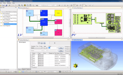
Particular attention in the 2021 release was given to fine-tuning the constraint and simulation capabilities in System Planner and Design Gateway, CR-8000’s engineering front-end applications. For 3D multi-board layout and routing, Design Force users benefit from the new place by area, template, and reuse functionality that enables the application of existing placement and routing patterns on new designs.
![]()
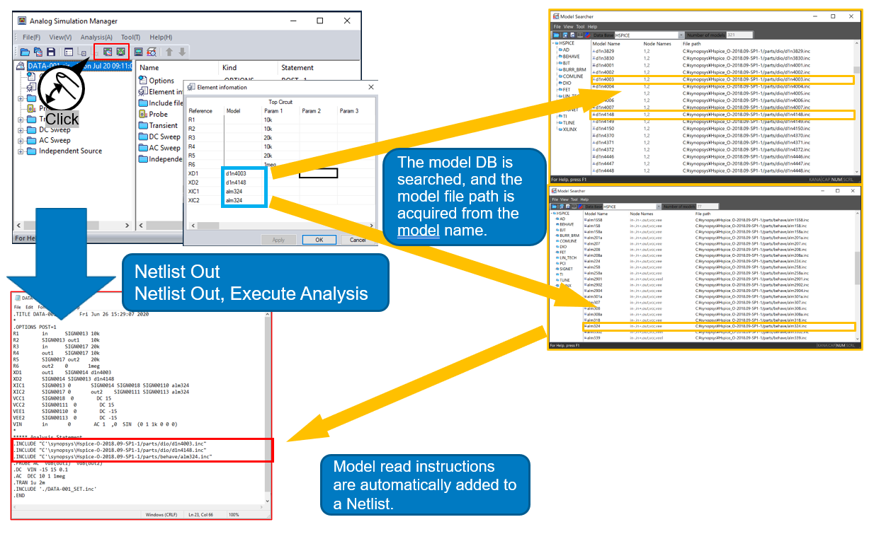
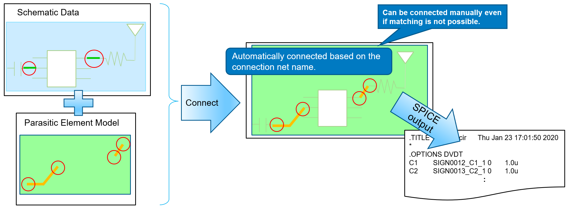
As part of the early analysis focus, Design Gateway now supports the simulation of PCB parasitic effects in the circuit design stage through the ability to include parasitic element models in SPICE simulations launched directly in the schematic. Circuit components and parasitic element models can be connected to create a SPICE model that incorporates parasitic elements.
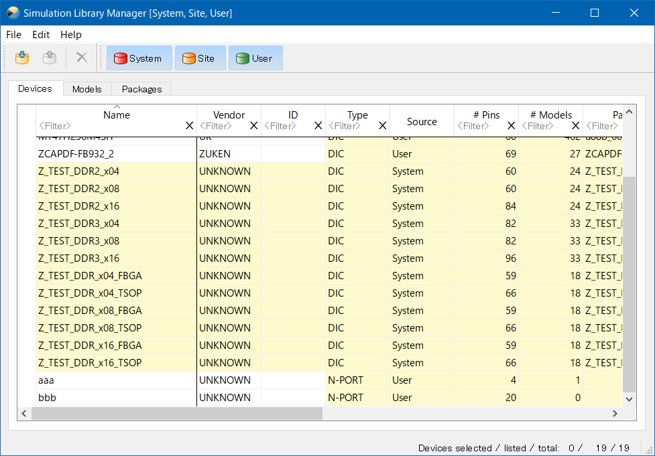
The simulation model library manager comes in a new, state-of-the-art user interface and is designed to handle today’s volume of model data smoothly. Importing models from various sources such as IBIS, SPICE, or S-Parameters is presented uniformly at the user’s fingertips.
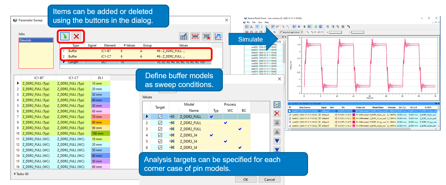
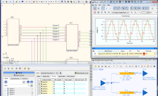
Signal integrity analysis functionality has been enhanced to support the execution of multiple pin models in one pass. A user can now explore a more extensive set of parameters in a reduced timeframe. It is now possible to analyze multiple pin models at once. Items can be added or deleted using the buttons in the dialog.
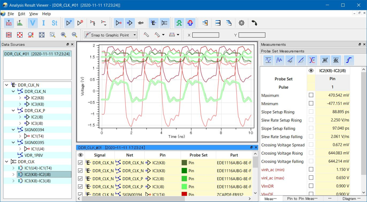
The SI verification of differential pair routing now reports measurement results of crossing voltages in both tables and waveform display. User productivity has been further improved by specifying automatic extraction and exporting of PI and EMI analysis results.
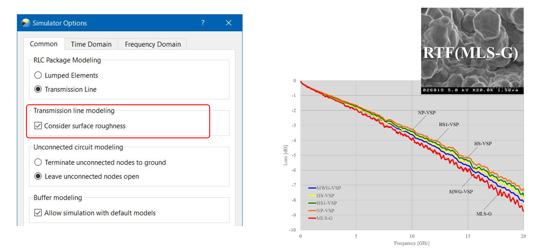
The SI Analysis now considers a more accurate model for the surface roughness of the copper PCB material
![]()
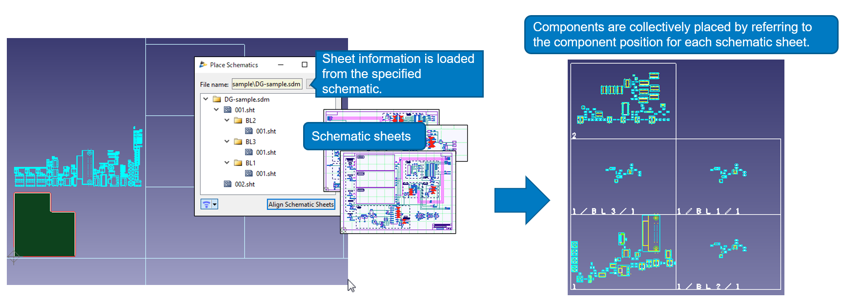
Components can be placed in Design Force by referring to the position on one of multiple schematic sheets. Sheet information is loaded from the specified schematic and components are placed in a batch operation by referring to the component position for each schematic sheet.
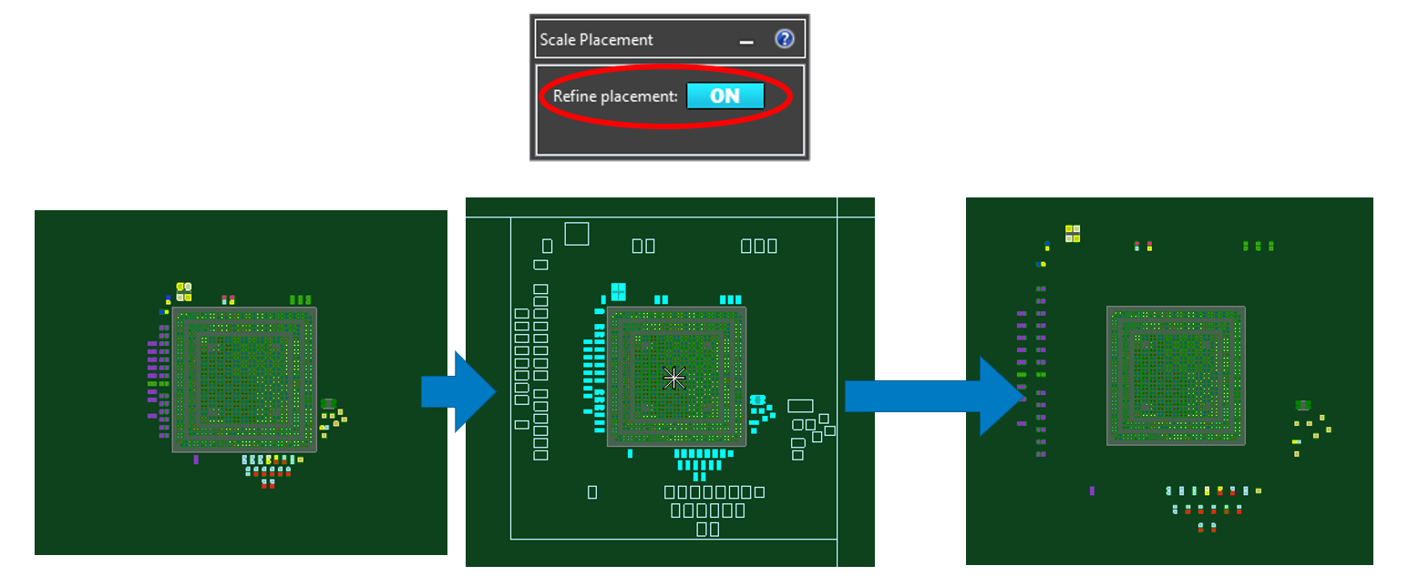
A new function automatically adjusts the spacing between components.When [Refine placement] is ON, overlapping with objects at the destination is cleared. The component positions are adjusted at once while the relative position between components is maintained.
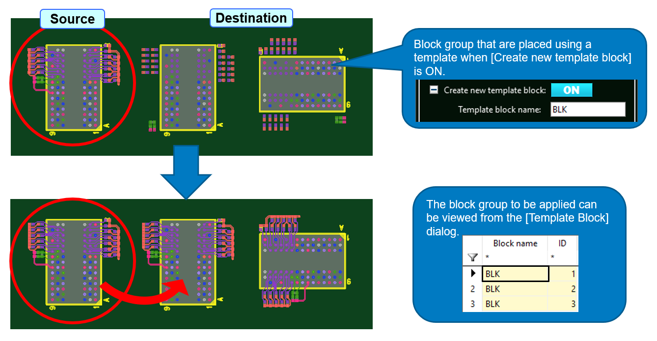
Edited placement and routing patterns can now be applied to another block among the blocks placed using a template. This new function enables PCB designers to create a template block and use the block to copy placement and routing. Blocks can be rotated while retaining their relationship to each other as well as the routing and vias.
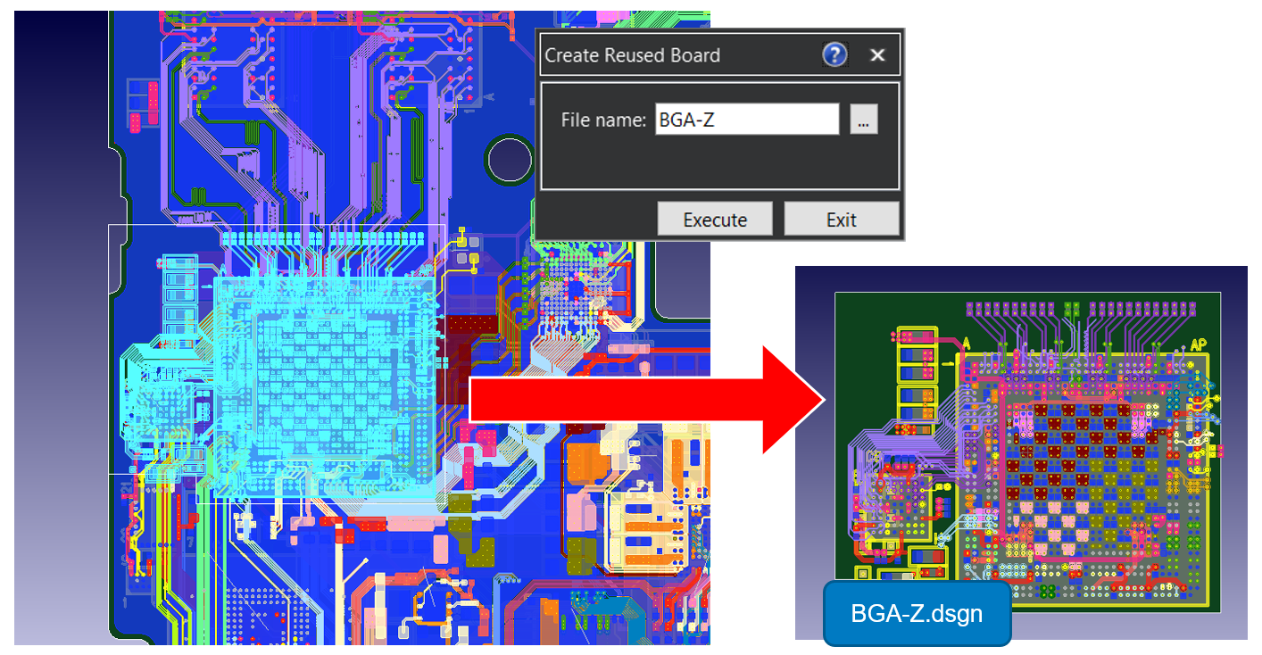
PCB designers can now easily generate a reuse board using the new Create Reused Board functionality by selecting an area of an existing design and saving it to a design file. You can then add this board to any design using Reuse Board. The placement of the components, as well as the routing, can drastically affect the performance of the circuit. By reusing a known-good circuit, you can be sure it will perform as expected–and save time and money on re-spins.
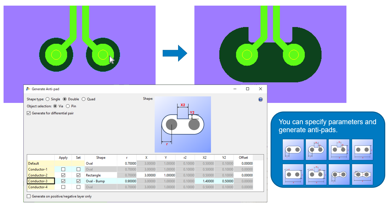
It is now possible to generate a cutout of a specific shape around vias and pins. An area fill can now be saved as a pad and its shape can be generated as an anti-pad. Having the ability to modify the clearance area between a via or pin and an internal plane can improve signal integrity. Anti-pad shapes can be saved in the PCB library for repeated use in the design.
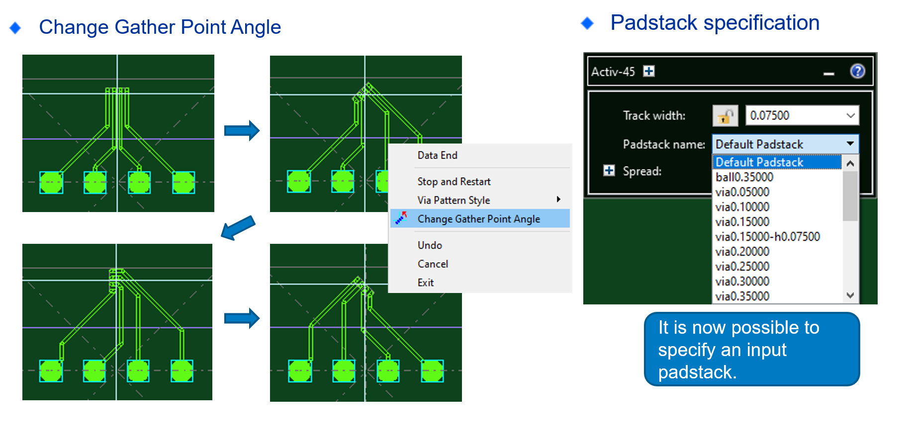
The functions and operability of the Intelligent Placement/Router command have been improved. It is now possible to change the angle at the route starting point of a trunk or bus from the assist menu. The routing and unrouting of track ends can now be executed as a batch operation Route Ends/Unroute Ends
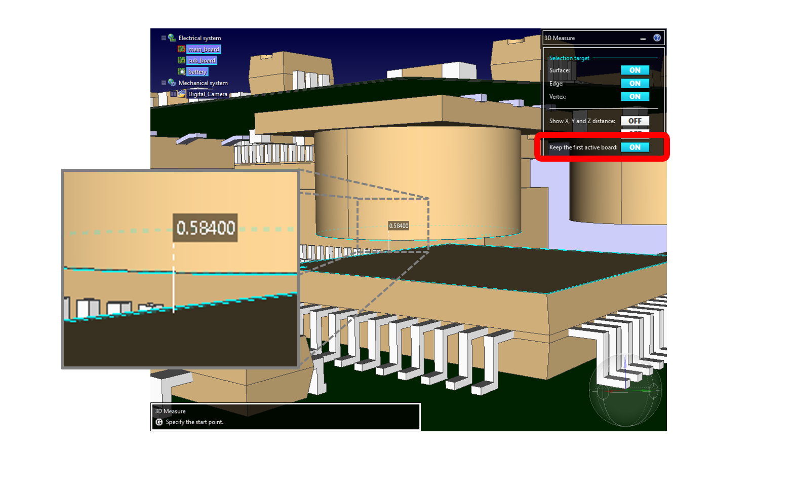
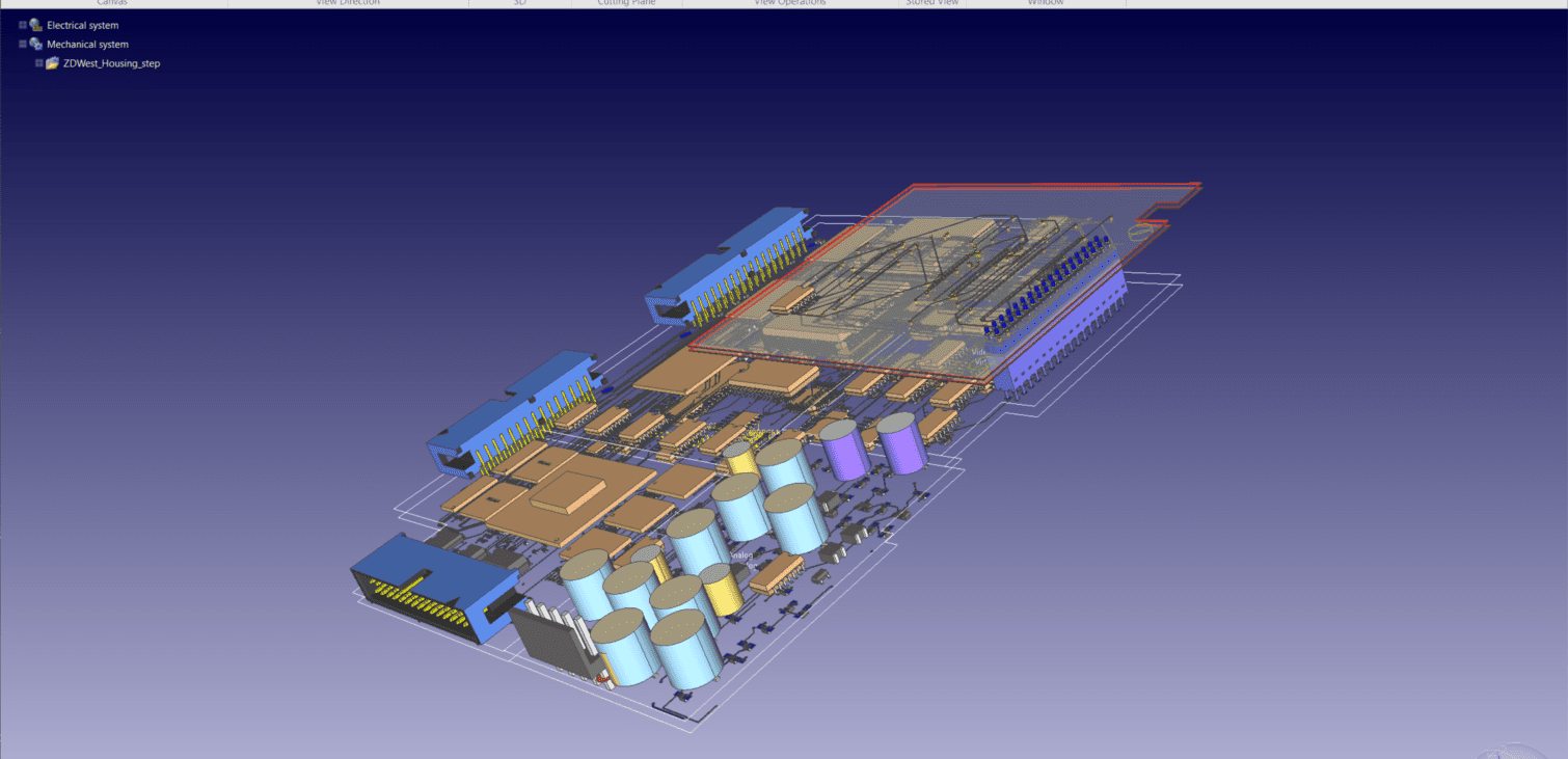
The 3D straight distance between different multi-boards can now be measured. The reference board can be fixed to make continuous measurements and the active board can be visually hidden from the canvas.
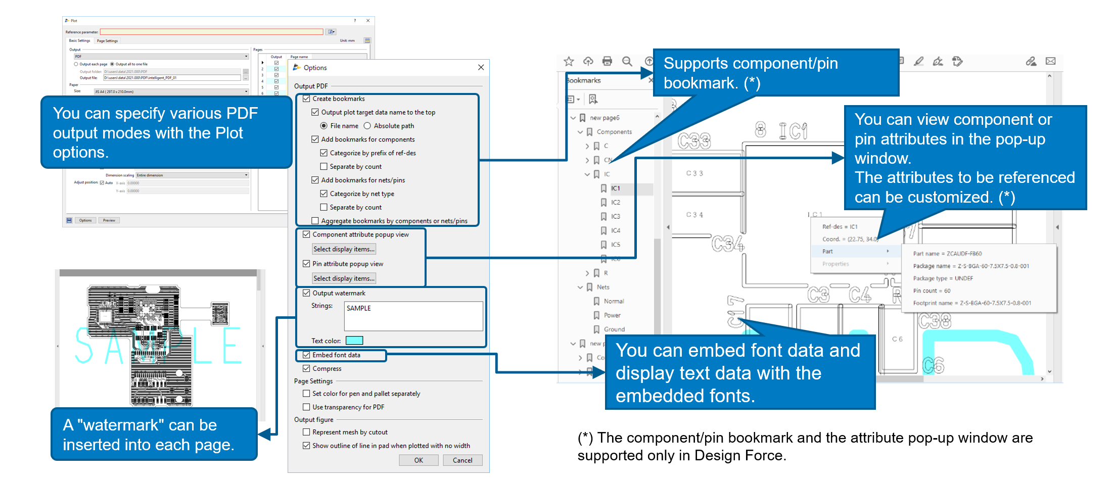
It is now possible to output a PDF file that enables a search by component or pin bookmark or a display of the attribute pop-up window. The Plot tool can generate an intelligent multi-page PDF directly from Design Force. The PDF output supports bookmarks as well as pop-up windows with net/component information. When a test technician needs to find a part or circuit on a board, the intelligent PDF can quickly show the location.
It is now possible to switch the output ON/OFF status of a non-electrical component. A component without terminals is judged to be a non-electrical component.
The following components can be excluded.
CR-8000 Design Force is the fastest, most effective PCB design solution available today. Design Force enables design teams to layout and verify their designs in the context of a complete system or product.
Design Force offers an intuitive, integrated environment for designing single and multi-die packages for wire-bond, flip-chip, and high density advanced IC packaging.
CR-8000 Design Gateway provides a platform for logical circuit design and verification of multi-board system-level electronic designs.
System Planner provides a system-level design environment for the architectural planning and optimization of electronic systems and products.